

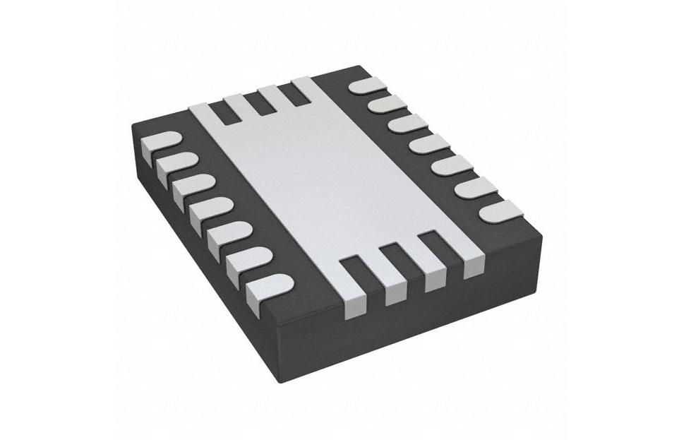
What Are the Key Features of RICHTEK RTQ2537GQV?
The RTQ2537GQV is a high-current, ultra-low-noise low-dropout linear regulator from Richtek Technology. It belongs to the RTQ2537 family and is offered in a compact VQFN-20L 3.5×3.5 package. The device is designed to deliver up to 4 A of output current while maintaining excellent noise and accuracy performance. This article examines its key features and explains why it is suitable for noise-sensitive and high-performance power rails.
1. Wide Input Voltage Range and Flexible Output Configuration
The RTQ2537GQV operates from a single input supply ranging from 1.1 V to 6.5 V, which simplifies power architecture design by allowing it to work with low-voltage rails directly.For output voltage, it offers two programming modes. The first mode supports 0.8 V to 5.5 V using an external resistive divider. The second mode supports 0.8 V to 3.95 V through pin-selectable settings via PCB layout, requiring no external resistors. This flexibility reduces component count and board space.
2. Ultra-Low Dropout Voltage
Dropout voltage is a critical parameter for LDOs, especially when the input and output voltages are close. The RTQ2537GQV achieves a maximum dropout of only 240 mV at 4 A output current, with a typical value of 110 mV at 4 A. This low dropout allows the regulator to maintain output regulation even when the input voltage drops close to the output level, improving efficiency and extending usable input range.
3. Excellent Noise and PSRR Performance
Noise-sensitive applications demand clean power rails. The RTQ2537GQV provides excellent noise immunity: 6.8 µVRMS at 0.8 V output and 10 µVRMS at 3.3 V output.It also achieves an ultra-high power-supply rejection ratio of 40 dB at 500 kHz, which minimizes the coupling of input supply noise to the output[reference:4]. An external bypass capacitor on the NR/SS pin further enhances output noise immunity. These features make it ideal for powering ADCs, DACs, VCOs, and RF components.
4. High Accuracy Over Line, Load, and Temperature
The device maintains 1% output voltage accuracy across line, load, and temperature variations. This tight tolerance ensures reliable operation for digital loads such as FPGAs, DSPs, and ASICs that require precise supply voltages. Remote sensing capability further improves regulation at the load point.
5. Protection and Control Features
The RTQ2537GQV integrates several protection and control functions. It includes an enable pin for external on/off control, a programmable soft-start function to reduce inrush current, and a power-good indicator for supply sequencing. Internal current limit and over-temperature protection safeguard the device under fault conditions. The output remains stable with a 47 µF or larger ceramic output capacitor. The device is fully specified over a junction temperature range of -40°C to 125°C.
Key Features Summary Table
| Feature | Specification |
|---|---|
| Input Voltage Range | 1.1 V to 6.5 V |
| Output Current | 4 A |
| Output Voltage Range | 0.8 V to 5.5 V (resistor divider); 0.8 V to 3.95 V (PCB layout) |
| Output Accuracy | 1% over line, load, and temperature |
| Dropout Voltage | 240 mV max at 4 A (typical 110 mV) |
| PSRR | 40 dB at 500 kHz |
| Output Noise | 6.8 µVRMS at 0.8 V; 10 µVRMS at 3.3 V |
| Protection Features | OCP, OTP, UVLO |
| Control Features | Enable, programmable soft-start, power-good indicator |
| Junction Temperature | -40°C to 125°C |
| Package | VQFN-20L 3.5×3.5 |
Questions and Answers
Q1: What is the main advantage of the RTQ2537GQV over standard LDOs?
A1: Its combination of 4 A output current, 240 mV maximum dropout, and 6.8 µVRMS noise makes it suitable for high-current, noise-sensitive rails where standard LDOs would either drop out too early or introduce excessive noise.
Q2: How does the device achieve low noise?
A2: It uses a low-noise reference and error amplifier, an NR/SS capacitor to filter reference noise, and a feed-forward capacitor to filter error amplifier noise. The high PSRR also prevents input noise from reaching the output.
Q3: What is the purpose of the power-good indicator?
A3: The open-drain PGOOD pin monitors the feedback voltage and signals when the output is within regulation. It helps with supply sequencing in multi-rail systems by allowing downstream devices to wait until the rail is stable.
Q4: What output capacitor is required for stability?
A4: The RTQ2537GQV is stable with a 47 µF or larger ceramic output capacitor. This large capacitance also helps maintain transient response during load steps.
Q5: What applications is this device best suited for?
A5: It is ideal for portable electronics, wireless infrastructure (SerDes, FPGA, DSP), and RF/IF components such as VCOs, ADCs, DACs, and LVDS drivers.Conclusion
The RTQ2537GQV combines high current capability, ultra-low dropout, excellent noise performance, and flexible output programming in a compact package. Its 1% accuracy and comprehensive protection features make it a robust choice for powering noise-sensitive analog and digital loads in demanding applications.